| |


Next: Transport Control Module
Up: Control Board
Previous: Fader Module
Contents
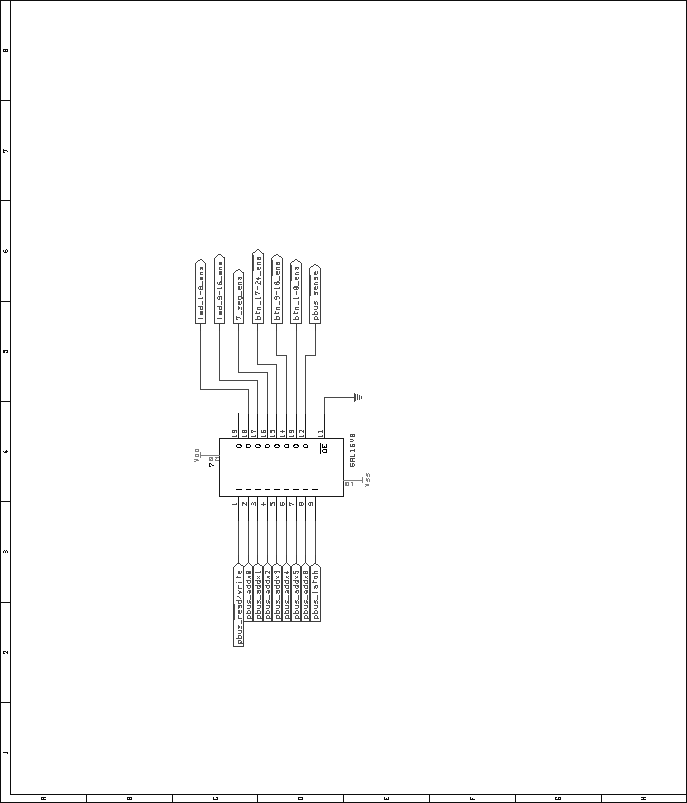
The output assign modules uses a 16V8 GAL for address decoding and enable
signal generation. Figure 44 shows the pin assignments
for the GAL used in the output assign module. The VHDL code used to
generate the GALs is included in the appendices, on page ![[*]](crossref.png) . .
Figure 44:
Output assign module, address decoding GAL.
 |
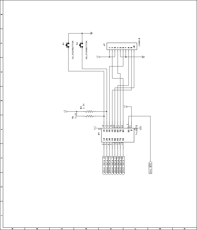
The status of 18 pushbutton switches need to be sensed by the
microcontroller. Many methods exist for connecting switches to a
microcontroller bus. To keep parts count and CPU use down, simple
latches are used to latch the status of eight switches at a time.
Firmware debouncing routines shall take the place of hardware
debouncing techniques. The
lack of a multiplexing scheme means less CPU time is wasted in reading
in the values of the switches, while the firmware debouncing routines
mean fewer components are used on the board. Figure 45
shows the circuit used to achieve these goals. Three of these
circuits are present, providing a total of 24 pushbutton inputs. Six
of these inputs are used for pushbuttons in the universal user
interface and cue stack sections of the control board.
Figure 45:
Output assign module, momentary pushbutton decoding schematic.
The output assign module uses three of these circuits, for a total decoding
capability of 18 on-board and 6 off-board buttons.
 |
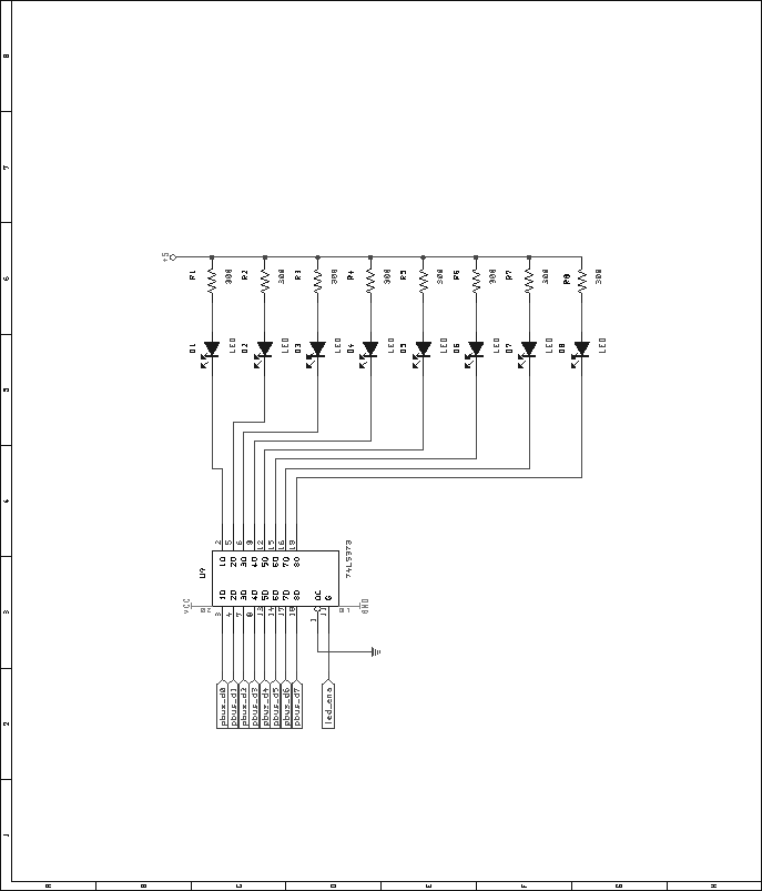
The output assign module contains several LED indicators that need to
be controlled by the microcontroller. A simple current-sinking scheme
involving 74LS373 octal latches is used, identical to that of the
fader module. Figure 46 shows the circuit.
Figure 46:
Output assign module, LED driver schematic. This module uses
two such circuits, for a total of 16 LEDs.
 |
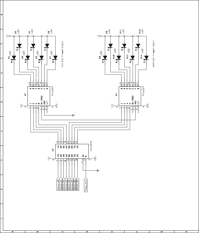
The output assign module contains a pair of 7-segment LED displays,
controlled by the microcontroller. While it certainly would have been
possible to drive the displays in a similar fashion to the bare LEDs
present on the same board, this was decided against due to the extra
Pbus ports needed. Instead, BCD-to-7-segment decoders were used,
with their inputs driven from a 74LS373 latch. Figure
47 shows the circuit used to drive the 7-segment
displays. Note the use of the ripple zero-blanking feature of the
74LS247 BCD-to-7-segment chips. This feature will blank both displays
when the a double-zero is displayed, and blank the leftmost display
when its value is zero.
Figure 47:
Output assign module, 7-segment display decoder and driver
schematic.
 |
Next: Transport Control Module
Up: Control Board
Previous: Fader Module
Contents
Steve Richardson
2000-07-06
|
Table of Contents
![[PDF]](/~prefect/images/pdficonsmall.gif) [Whole document in PDF 1.9MB]
[Whole document in PDF 1.9MB]
[more photos and information]
|