| |


Next: Output Assign Module
Up: Control Board
Previous: Control Board
Contents
Two fader modules are present in the prototype control board. They
are identical boards with different GAL programming and jumper
settings.
Figure 71 shows the silkscreen/assembly layer for the
fader board. Table 2 shows the bill of materials
for a single fader board. Figures 72 and
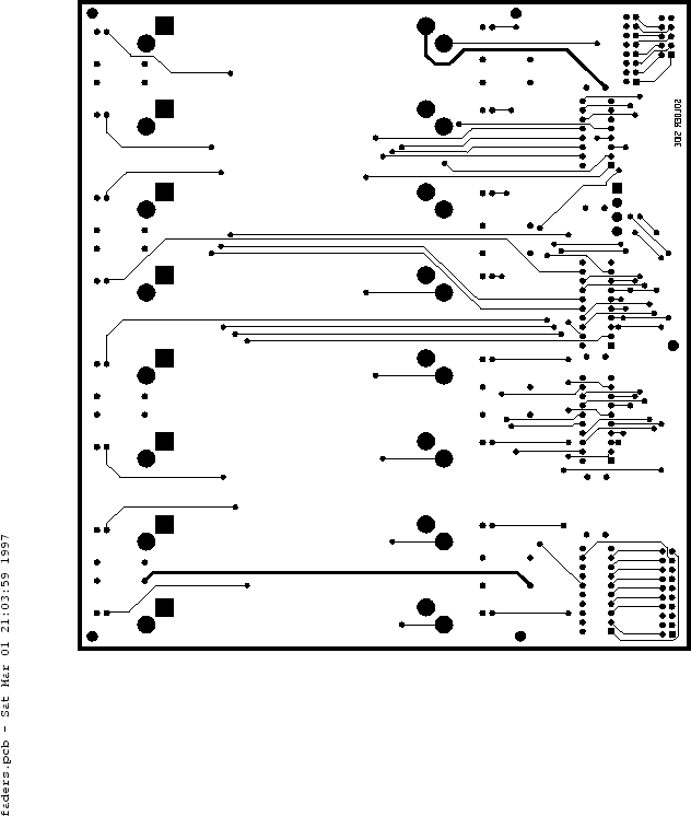
73 show the top and bottom routing layers, respectively.
Figure 71:
Fader module PCB, silkscreen/assembly drawing.
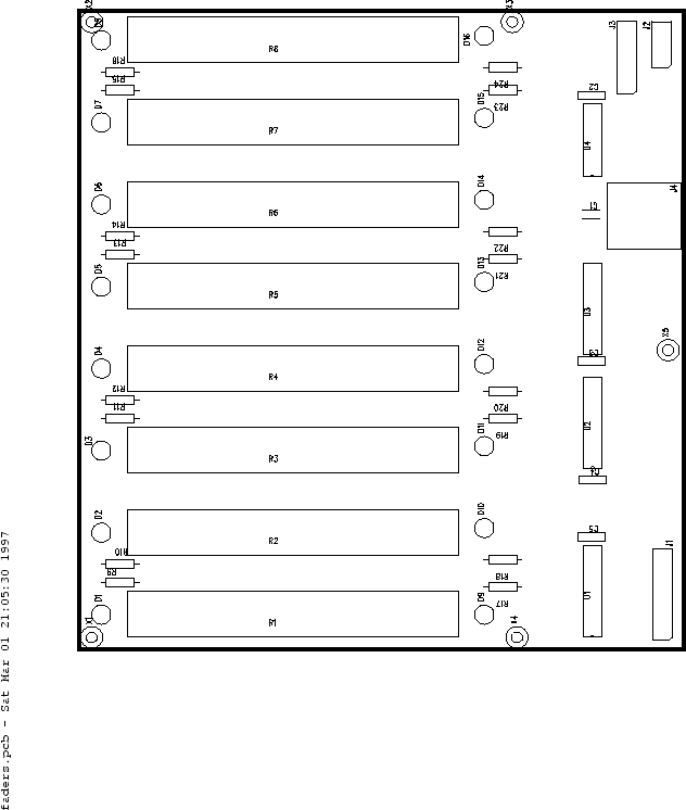 |
Table 2:
Fader module, bill of materials.
| REFDES |
QTY |
DESCRIPTION |
| R1 - R8 |
8 |
ALPHA 500K slide potentiometer |
| R9 - R24 |
16 |
300 ohm 1/8W |
| C1 |
1 |
10uF electrolytic |
| C2 - C5 |
4 |
0.1uF monolithic |
| D1 - D8 |
8 |
Green T1-3/4 LED |
| D9 - D16 |
8 |
Red T1-3/4 LED |
| U1 |
1 |
GAL16V8 |
| U2, U3 |
2 |
74LS373 |
| U4 |
1 |
CD4051 |
| J1 |
1 |
20-pin DIP header |
| J2 |
1 |
10-pin DIP header |
| J3 |
1 |
16-pin DIP header or wire jumper |
| J4 |
1 |
4-pin 0.156in. power connector |
|
Figure 72:
Fader module PCB, component-side routing.
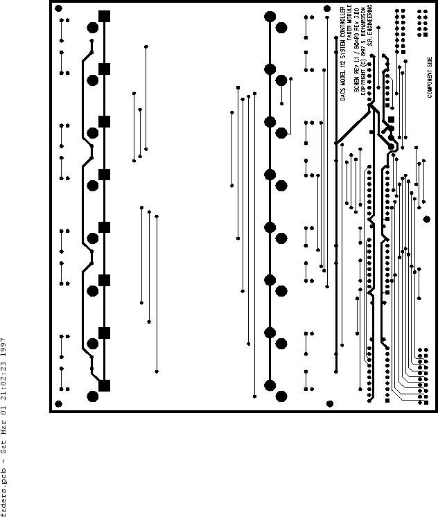 |
Figure 73:
Fader module PCB, solder-side routing.
 |
Next: Output Assign Module
Up: Control Board
Previous: Control Board
Contents
Steve Richardson
2000-07-06
|
Table of Contents
![[PDF]](/~prefect/images/pdficonsmall.gif) [Whole document in PDF 1.9MB]
[Whole document in PDF 1.9MB]
[more photos and information]
|